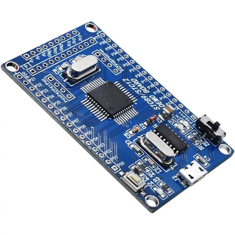
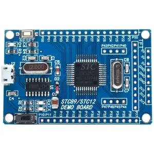
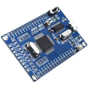
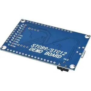
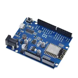
Features:
- High speed, 1 clock/machine cycle, enhanced core, 6~12 times faster than ordinary 8051.
- Wide voltage: USB port 5V IO level is 5V.
- Add the second reset function pin /P4.6 (high reliability reset, adjustable reset threshold voltage and frequency), this function is not needed when it is less than 12MHz.
- Increase the external power failure detection circuit/P4.6, which can save the data into EEPROM in time when the power is off, and there is no need to operate the EEPROM during normal operation.
- Low power consumption design, idle mode (can be awakened by any interrupt).
- The pins that support power-down wake-up, P3.2/INTO, P3.3/INT1,TO/P3.4, T1/3.5, RXD/3.0, P1.3/CCPO (or P4.2/CCPO), P1.4/CCP (or P4.3/CCP1), EX-LVD/P4.6.
- Operating frequency: 0~35MHz, equivalent to ordinary 8051:0~420MHz
- Clock: external crystal or internal R/C oscillator is optional, set when downloading and programming user program by ISP.
- 8/16/32/40/48/56/60/62K bytes on-chip Flash program access device, erasing and writing times more than 100,000.
- 1280 bytes on-chip RAM data memory.
- Large-capacity on-chip EEPROM function, erasing and writing more than 100,000 times.
- ISP/1AP, programmable in system/programmable in application, no programmer/emulator required.
- 8-channel, 10-bit high-speed ADC, speed up to 250,000 times per second, 2 PWM can also be used as 2 D/A.
- 2-channel capture/compare unit (CCP/PCA/PWM), which can be used to realize 2 timers or 2 external interrupts (support rising edge/falling edge interrupt).
- 2 16-bit timers (compatible with ordinary 8051 timer TO/T1), 2 PAC can realize 2 more timers.
- Programmable clock output function (TO outputs clock at P3.4, T1 outputs clock at P3.5, BRT outputs clock at P1.0).
- Hardware watchdog (WDT).
- Single baud rate generator.
- SPI high-speed synchronous serial communication interface.
- Dual serial ports, full duplex asynchronous serial port (UART), compatible with ordinary 8051 serial time division multiplexing, can be used as 3 groups.
- Advanced instruction integration structure, compatible with ordinary 8051 instruction set, with hardware multiplication/start instructions.
- General |/O (36/40/44), after reset, it is: quasi-bidirectional port/weak pull-up (normal 8051 traditional 10) can be set to four modes: quasi-bidirectional port/weak pull-up, strong push/strong The pull-up is only input/high-impedance, open-drain. Each IO port can drive up to 20mA, but it is recommended that the entire chip should not exceed 120mA.
Note:
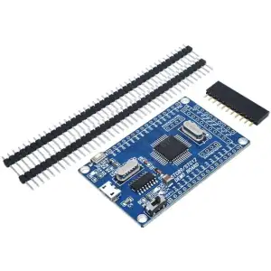
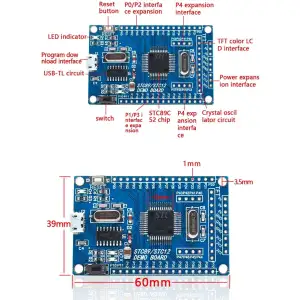
- Use USB Micro data cable to provide power supply and program download, need to be purchased separately.
- All pin headers are not welded, which is convenient for your DIY, please be aware.
About the PO port pull-up resistor problem:
When you are using the STC89C52 version, if the PO port is used for external output driving, an external pull-up resistor is required. It is used as a general LCD bus such as LCD1602 and LCD12864. It can be used directly without an external pull-up resistor.
| POM0[7:0] | POM0[7:0] | I/O Mode |
| 0 | 0 | Quasi-bidirectional port (traditional 8051 IO mode), the sink current can reach 20mA and the source current is 230uA. Due to manufacturing errors, it is actually 160~250uA. |
| 0 | 1 | Push-pull output (strong pull-up output, up to 20mA) |
| 1 | 0 | Input only (high impedance) |
| 1 | 1 | Open drain, the internal pull-up resistor is disconnected, and an external |


Reviews
There are no reviews yet.